Design Menu
Check Current Layer
This command causes the Osmond system to perform a clearance check of all traces on the current layer. If any clearance conflicts are found, the affected paths and/or pads are highlighted and the dialog as shown below appears.
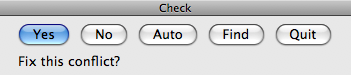
If the conflict is not visible, press the Find button. This pans the view to bring the area of the conflict to the center of the screen. If you press No, the conflict will be skipped and the next conflict (if any) will be found and highlighted. If you press Quit, the check will be aborted and the dialog will disappear. If you press Auto, the Osmond system will attempt to resolve all conflicts automatically by moving connecting paths without further dialog. If you press Yes, the Osmond system will attempt to find a solution to the conflict and will display that solution highlighted while changing the dialog as shown below.
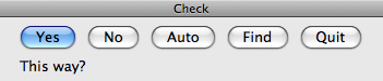
If you press Yes, the proposed solution will be implemented and the system will move on to the next conflict (if any). If you press No, the proposed solution will not be implemented and the system will attempt to find and present a different solution for your approval. If you press Auto, the proposed solution will be implemented and the system will attempt to resolve all remaining conflicts automatically without further dialog. If you press Quit, the proposed solution will not be implemented, the dialog will disappear, and all remaining checks will be aborted.
Check All Layers
The Check All Layers command is similar to the Current Layer command above. The All Layers command, however, performs a clearance check of all layers of the design.
Find Overlapping Holes
The Find Overlapping Holes command searches the design for two or more holes that overlap. This is usually the result of an error in the design and should normally be corrected. If a pair of overlapping holes is found, the view is moved to position the holes exactly in the center. You may need to increase the magnification to make it more obvious which holes are exactly in the center. If there are no overlapping holes, an alert will so indicate.
Find Multiple Thermal Connections
The Find Multiple Thermal Connections command searches the design for pins that have thermal connections on more than one layer. This may indicate a design error that could potentially tie two different signals together (like power and ground). If a pin with multiple thermal connections is found, it is centered in the display. If no pins with multiple thermal connections are found, an alert will so indicate.
Find Conflicting Pins
The Find Conflicting Pins command searches the design for pins whose pads are closer together than the default spacing, and whose signals differ. If a pin is found too close to another pin, an alert so indicates and the pin is centered in the display. If no pin is too close to another pin, an alert will so indicate.
Check All Connections
The Check All Connections command checks that all signals specified in the pin list are fully connected and that there are no cases in which two different signals are connected together. This test is more exhaustive than the Check All Layers command above in that it examines in detail both copper traces and copper flooded areas such as signal planes or ground planes. In particular, it can find problems in which two or more signals are connected to the same signal plane. It can also find cases in which pins that should be connected through a signal plane are actually not connected due to the isolation of one portion of the signal plane from another. However, the Check All Layers command does perform clearance checks while this command does not.
Because this test is so exhaustive, it requires a large number of processing cycles. Depending on the size of the design and the speed of the computer, this test may take several minutes to complete.
If no problems are found, an alert so indicates. If a problem is found, an alert appears that lists the nature of the problem and the pin where the problem was detected. Also, the view is moved to position the pin at the center. Because connection problems may originate far away from where they are detected, you should treat the location of pin as just a starting place to look.
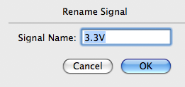
Rename Signal…
The Rename Signal command brings up the dialog as shown in below to allow you to rename the current signal.
Next Signal
The Next Signal command cycles through the Net List in order and selects the next signal that remains unconnected. Pins belonging to this signal are highlighted and the signal name is shown at the top left message area. The command can also be issued by pressing the letter N on the keyboard.
Previous Signal
The Previous Signal command cycles through the Net List in reverse order and selects the nearest previous signal that remains unconnected. Pins belonging to this signal are highlighted and the signal name is shown at the top left message area. The command can also be issued by pressing the letter V on the keyboard.
Make Signal Plane…
The Make Signal Plane command brings up the dialog as shown below to allow you to specify whether or not the current layer is a (reversed image) signal plane layer, and if it is a signal plane layer, to specify various initial values.
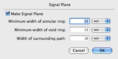
If you wish the current layer to be a signal plane layer, check the Signal Plane check box. If the current layer is already a signal layer and you wish to change it back to a normal layer, uncheck the Signal Plane check box.
The Osmond system uses patterns of reverse image pads and paths to control whether or not a pin is connected to the ground or signal plane. In the image below, the blue area shows where copper remains on the layer while the white area shows where copper is removed from the layer. Light blue circles at the center of each pad show where there is a hole for a through-hole pin.

In the first pattern, a reverse image pad (called a void pad) removes the copper from around the through-hole pin. This causes the pin to be completely isolated from the copper plane. The Minimum Width of Void Ring field allows you to specify the minimum width of the copper-free area surrounding the hole.
In the second pattern, eight reverse image paths surround the hole leaving an area of copper in an octagon shaped annular ring. The pin connects to the copper in the annular ring but is still isolated from the copper plane. The Minimum Width of Annular Ring field allows you to specify the minimum width of the octagon shaped copper ring surrounding the hole, while the Width of Surrounding Path field allows you to specify the width of the reverse image paths surrounding the ring.
The third pattern is like the second except two of the surrounding paths have been removed. Now, the pin is connected to the copper in the annular ring and also connected to the copper plane through passages at the top and bottom of the pin. If we were to remove all the surrounding paths, the pin would still be connected to the copper plane but soldering the pin would be more difficult because of the large heat sink provided by the copper. The surrounding paths therefore act as thermal barriers to permit easier soldering.
The fourth pattern is similar to the third except two different surrounding paths have been removed to provide diagonal connecting passages to the copper plane.
When you make a signal plane on an inner layer, all pads belonging to the current signal will be converted to the second pattern while all pads that do not belong to the current signal will be converted to the first pattern. On an outer layer, however, all pads are converted to the second pattern.
For example, to make a ground plane on an inner layer, go to that layer and select the ground signal with the Connect tool by clicking on any pad that belongs to ground. Then make the layer a signal layer with the Make Signal Plane… command. Now you can connect any of the ground pads to the copper plane by using the Thermal tool to convert pads from the second pattern to the third pattern or fourth pattern or any other pattern that you choose.
Make Moat
The Make Moat command requires that one (and only one) closed path be selected. A closed path is a path in which the beginning of the path is at the same point as the end of the path.
The Make Moat command creates a pattern of closed freehand paths that completely surround all pads and traces within the currently selected closed path. This command is usually a prelude to the Paint command described below.
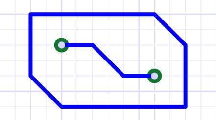
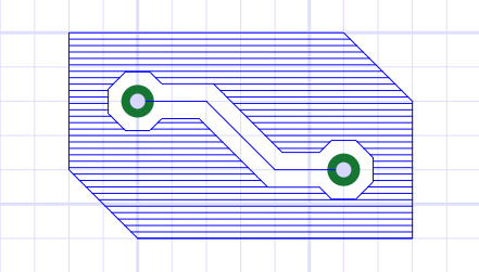
For example, given two pads connected by a path within a closed path as shown in below.
If we select the enclosing path we can now invoke the Make Moat command to produce the result below.
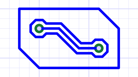
The widths of all new paths are the same as the width of the original selected path, and the spacings permitted by the new paths are equal to the spacing of the original selected path.
Paint
The Paint command allows you to fill an area with copper. The area to be filled is defined by a closed path. However, any closed areas within the selected closed area will be avoided.
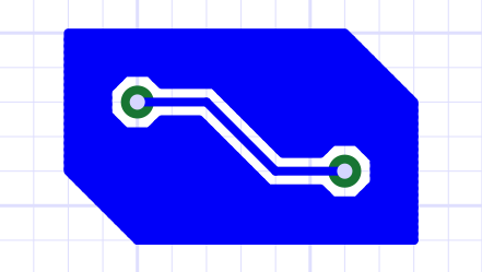
Let us take, for example, the circuit pattern below consisting of a closed freehand path surrounding another closed path which in turn surrounds two pads connected by a path.
If we select the outer path, we can now invoke the Paint command to produce the result below.
Paint works by drawing horizontal paths. To see this more clearly, you can turn off Full Width Traces in the View menu. The result is shown below.
Horizontal paths are drawn with the same width as the surrounding path. Also, the spacing between paths is determined by the spacing of the surrounding path. To produce solid copper, the spacing of the surrounding path should be set to zero. If the spacing is not set to zero, you will get gaps between paths.
Make Moat and Paint represent historically early approaches to creating local ground plane areas. For many situations, however, you may be able to achieve superior effects by using the newer Copper Flood and Selected Paths Flooded commands described below.
Copper Flood
The Copper Flood command is a toggle command that turns on and off Copper Flood for the current layer. A layer with Copper Flood on is solid copper except for clear space surrounding each pad and each path. The amount of clear space surrounding each pad is determined by the default spacing of the current layer, modified by the spacing adjust of the pad itself. The amount of clear space surrounding each path is determined by the spacing of the path.
The copper is made visible on the screen whenever Full Width Paths is turned on in the View menu. However, it is drawn semi-transparently to allow features on other layers to show through.
This command can be used to create a ground or power plane on the current layer with the added ability to have embedded paths. Such paths, having non-zero spacing, are isolated from the copper plane. Use the Thermal Tool to create connections from pads to the copper flood area.
You can selectively remove copper in an area by drawing a path that has zero width but non-zero spacing. Because the width is zero, the path itself does not contribute any copper but the spacing causes some of the copper in the flooded region to be removed. You can also use the Paint command, using a zero-width and non-zero-spacing surrounding path, to remove larger areas of copper.
Copper Flood and Make Signal Plane… are alternate, mutually incompatible techniques for creating a signal-plane or ground-plane. Because of this, Copper Flood is disallowed on signal-plane layers.
Selected Paths Flooded
The Selected Paths Flooded command is a toggle command that turns on and off Copper Flood for an area of the board that is defined by a selected freehand path. This produces an area of the board similar to that created by the Copper Flood command above, but on a smaller and more precise scale.
Before using this command, define a region by drawing a closed path with the Draw Freehand Path tool. Then select this path with the Select / Move Parts tool and issue the Selected Paths Flooded command to turn on Copper Flooding for the region. If you select a path that already defines a Copper Flood region, the Selected Paths Flooded command will turn off Copper Flooding for that path.
Flip Over
The Flip Over command causes the entire design to flip over so that the back side of the board is now the front and the front side is now the back. Issuing the command a second time restores the design to its original state.
Dup Layer Before
The Dup Layer Before command creates a new layer by duplicating the current layer and placing it before the current layer. All pads are duplicated but none of the paths.
Dup Layer After
The Dup Layer After command creates a new layer by duplicating the current layer and placing it after the current layer. All pads are duplicated but none of the paths.
Add Inner Layer
The Add Inner Layer command creates a new inner layer and places it just before the last layer. Unlike the Dup Layer Before or the Dup Layer After command, this works correctly even if there is not already an inner layer to duplicate.
Delete Layer
The Delete Layer command deletes the current layer with all its pads and paths. This reduces the total number of layers by one.
Prune Library
The Prune Library command removes from the part type library, all part types that are not in use. If you import a large library and use only a few part types, this command may significantly reduce the size of your design file.
Make Rats Nest
The Make Rats Nest command creates a rats nest of paths on the Rats Nest layer connecting pins belonging to every signal in the design. Paths in the rats nest can then be used by various tools, such as the Quick Route tool and the Wrap Path tool, to route paths on real board layers.
Destroy Rats Nest
The Destroy Rats Nest command eliminates all paths in the Rats Nest layer.
Make One Rats Nest
The Make One Rats Nest command creates a rats nest of paths on the Rats Nest layer connecting all pins belonging to the current signal. The current signal is usually selected using the Choose/Connect tool. You can also make a rats nest of one signal using the Choose/Connect tool by clicking on a pin while pressing the Option key.
Destroy One Rats Nest
The Destroy Rats Nest command eliminates all paths in the Rats Nest layer connecting pins that belong to the current signal.